
Solar panels are made of silicon solar cells sealed between tempered glass in front and a polymer backsheet or second sheet of glass behind. A plastic encapsulant (EVA or POE) bonds the stack, silver and copper carry the current, an aluminum frame holds everything, and a junction box on the back connects it to your system. Silicon is the main semiconductor in conventional panels, but glass is the heaviest material, at roughly three quarters of a typical panel.
That answers what a solar panel is made of, but not why each layer exists. This guide from AGHow walks through the stack layer by layer, starting at the side that faces the sky. It then explains what solar cells and PV cells are made of, how monocrystalline, thin film, TOPCon and heterojunction designs differ, which materials raise health or environmental questions, how panels are manufactured, and what can be recycled.
What Are Solar Panels Made Of?
A conventional solar panel is a laminated stack of glass, polymer film, silicon cells and metal, finished with an aluminum frame and an electrical box. To understand what a solar panel is made of, it helps to separate three groups of materials:
- Solar cell materials: silicon, the small amounts of boron and phosphorus that make it a working semiconductor, thin surface coatings and metal contacts.
- Solar module (panel) materials: glass, encapsulant films, a backsheet or rear glass, and the ribbons that connect cells.
- Structural and electrical components: the aluminum frame, junction box, bypass diodes, cables and connectors.
A solar cell is only the part that converts light into electricity. A solar panel, also called a module, is a finished product that protects many cells and makes them usable. Panel construction varies by manufacturer and design, so the table describes a typical framed crystalline silicon panel.
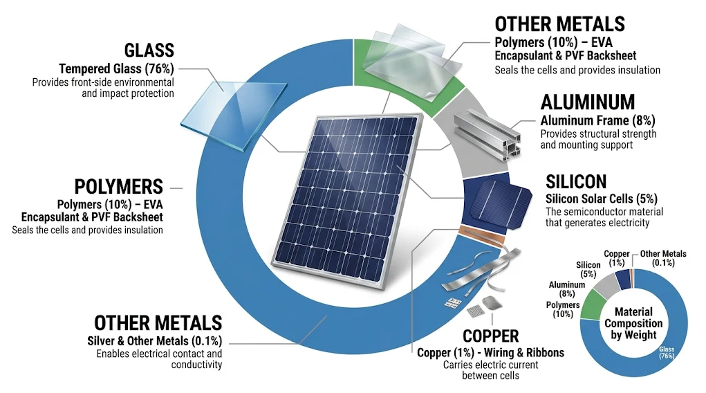
| Component | Main material | Primary function |
|---|---|---|
| Front cover | Tempered glass | Protects the cells while letting light through |
| Solar cells | Crystalline silicon | Convert sunlight into electricity |
| Encapsulant | EVA or POE | Bonds the layers and protects cells from moisture and shock |
| Conductive contacts | Silver and copper | Collect and carry electricity |
| Rear cover | Polymer backsheet or glass | Protects the back and insulates electrically |
| Frame | Aluminum | Gives structural support and mounting points |
| Junction box | Plastic enclosure with electrical parts | Houses connections and bypass diodes |
By weight, the picture looks different. The figures below come from one study reported by MET, and they are typical, not universal.
| Material | Typical share of panel weight |
|---|---|
| Glass | About 76 percent |
| Polymer (encapsulant, backsheet, junction box) | About 10 percent |
| Aluminum | About 8 percent |
| Silicon | About 5 percent |
| Copper | About 1 percent |
| Other metals, including silver, tin and lead | About 0.1 percent |
The EPA agrees that glass makes up about 75 percent of a panel. The semiconductor that does the work is a small share of the weight.
Solar Panel Construction: A Layer by Layer Breakdown
In a typical framed crystalline silicon panel, the layers run from the sunny side to the back: glass, front encapsulant, solar cells, rear encapsulant, then a backsheet or rear glass. The frame surrounds the stack, and the junction box sits on the back. Each layer below answers the same questions: what it is, why it is used and what it does.
1. Tempered Glass: The Protective Front Layer
The front layer is tempered glass, which is glass that has been heat treated to make it much stronger than ordinary glass. It protects the cells from rain, wind blown debris, dust and hail, while letting sunlight through.
Solar panels use glass with high transparency because any light absorbed or reflected by the glass is light the cells never receive. Even very clear glass reflects some sunlight. Aurora Solar, citing a study in the journal Solar Energy, says this can reduce the light reaching the cells by around 4 percent, which is why many panels add a thin antireflective coating to the glass surface.
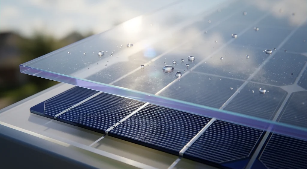
Glass quality matters for both performance and durability. High transmission raises output, while strength and surface quality affect how well a panel survives decades of weather. Glass is also the largest share of panel weight, which makes it the main material to recover at end of life.
2. Encapsulant Layer: EVA and POE
EVA stands for ethylene vinyl acetate, and POE stands for polyolefin elastomer. Both are transparent polymer films that wrap the solar cells. Aurora Solar describes EVA as the most common choice because it is flexible, durable and low cost, and POE as common in many higher performance panels for added durability.
The encapsulant is more than glue. Sheets of film are placed above and below the cells, and during lamination, heat and vacuum melt them so they bond to the glass, the cells and the rear layer. The result is a sealed, solid assembly.
It does four jobs:
- Bonds the layers into one unit.
- Cushions the thin, brittle cells against mechanical stress.
- Limits moisture reaching the cells and contacts.
- Electrically insulates the cells while staying clear enough for light to pass.
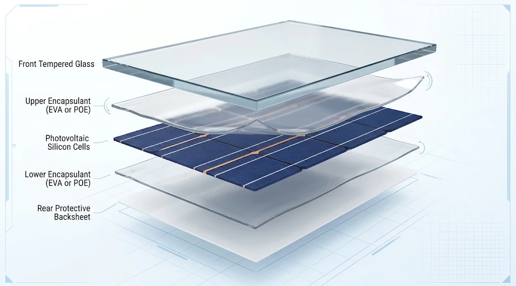
Which encapsulant a panel uses depends on the manufacturer and the cell design. POE is generally valued for lower moisture permeability than standard EVA, which can matter for cell designs that are more sensitive to moisture.
3. Solar Cells: The Silicon Semiconductor Layer
Photovoltaic (PV) cells, also called solar cells, contain a semiconductor that absorbs sunlight and converts it into electricity. The DOE explains that a semiconductor conducts electricity better than an insulator but not as well as a metal, and that not every semiconductor can convert light to electricity.
Why silicon? Silicon is by far the most common semiconductor in solar cells. The DOE notes it is the second most abundant element on Earth after oxygen and is also the most common semiconductor in computer chips. In crystalline silicon, atoms join in an orderly lattice, which makes converting light to electricity more efficient. The DOE says silicon cells currently offer a combination of high efficiency, low cost and long lifetime, with modules expected to last 25 years or more and still produce over 80 percent of their original power.
From sand to wafer. The DOE describes the main steps for silicon cells:
- Quartz is refined into polysilicon, a high purity form of silicon, commonly by the Siemens process.
- For monocrystalline silicon, a large cylindrical crystal ingot is grown by the Czochralski process, where a small seed crystal is touched to molten silicon and slowly pulled upward.
- The ingot is sliced into very thin wafers with diamond coated wire saws.
- The wafer surface is chemically textured, which removes saw damage and helps more light enter.
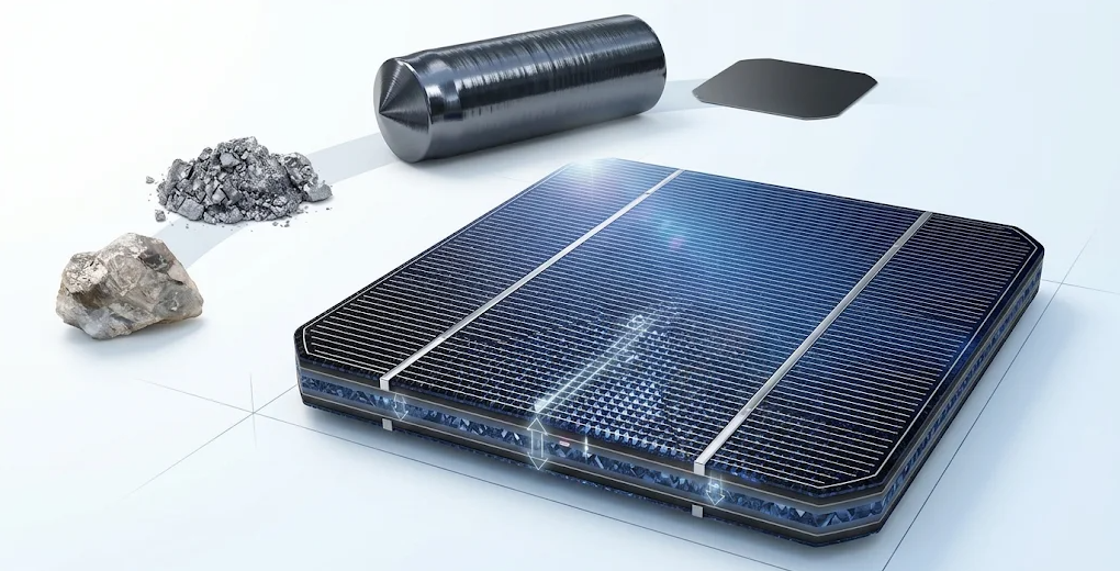
Doping and the p n junction. Pure silicon is not enough. Manufacturers add tiny amounts of other elements, a process called doping. Boron makes silicon p type, which has a shortage of electrons. Phosphorus makes it n type, which has extra electrons. Where a p type region and an n type region meet, they form a p n junction with a built in electric field.
When sunlight is absorbed, its energy frees electrons. The built in field pushes them in one direction, so they flow as a current through the metal contacts to an outside circuit. The cells and the panel produce direct current (DC) electricity.
Monocrystalline versus polycrystalline. Monocrystalline cells are cut from a single, continuous crystal, which gives them a uniform dark appearance and generally higher efficiency. Polycrystalline cells come from silicon that solidified into many crystal grains, which was once cheaper but less efficient. Today monocrystalline wafers dominate. The ITRPV industry roadmap says monocrystalline silicon accounts for almost the entire crystalline silicon wafer market.
Not all solar cells use crystalline silicon. Thin film cells use layers of other semiconductors, such as cadmium telluride, deposited on glass, plastic or metal, as covered later in this guide.
4. Metal Contacts, Busbars and Copper Ribbons
Electricity leaves the cell through thin metal lines printed on its surface. The thinnest lines, called fingers, collect current across the cell. Thicker lines called busbars gather current from the fingers. The DOE describes these as the grid like lines on a cell that extract current. Most crystalline silicon cells use screen printed silver paste for this, a method the DOE calls very common.
Copper ribbons, which are flat strips of copper, then link the front of one cell to the back of the next, so the cells are joined into strings. Wiring cells in series adds their voltages together, which is how a panel reaches a usable voltage.
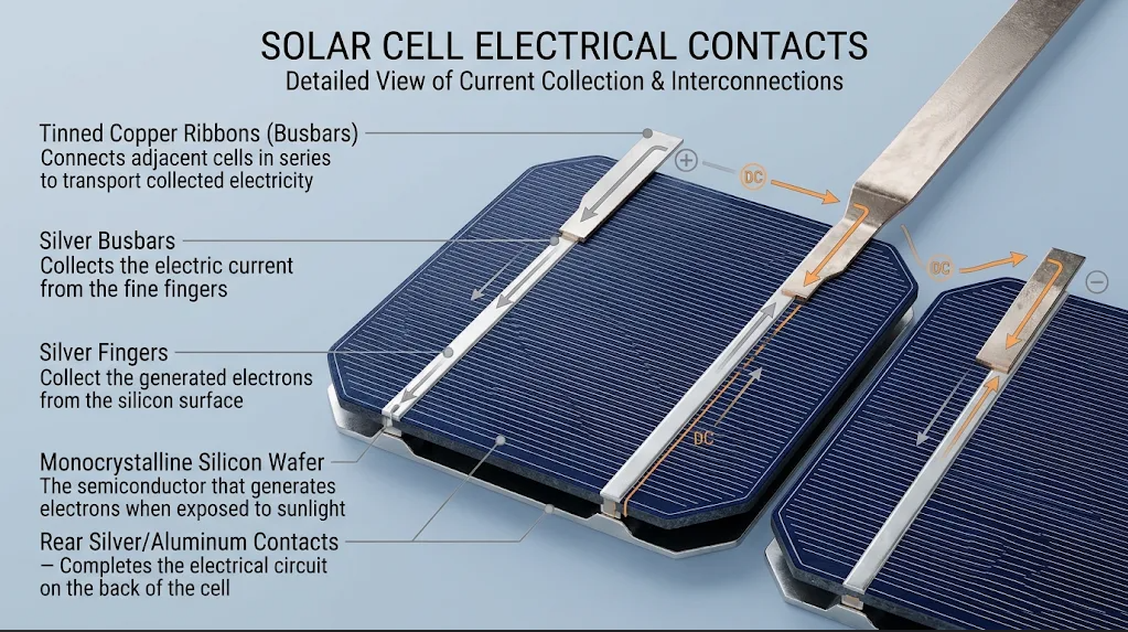
Silver is used because it conducts electricity better than other metals, which keeps resistance losses low. There is a trade off: metal lines also shade the cell, so designers want them as thin as possible while still conducting well.
Metallization is not identical across panels. According to the ITRPV roadmap, as reported by TaiyangNews, an M10 size cell used about 70 mg of silver for PERC, 88 mg for TOPCon and 100 mg for heterojunction in 2025. TOPCon and heterojunction cells need silver on both sides, while older PERC cells used aluminum on the rear. Manufacturers are cutting silver with finer printed lines, multi busbar layouts and busbarless designs. In the laboratory, Fraunhofer ISE reported silver use of about 1.1 mg per watt peak using electroplated contacts, compared with 10 to 12 mg per watt in current production. That is a research result, not what every panel uses today.
5. Rear Encapsulant Layer
Behind the cells sits a second encapsulant film, usually the same kind of polymer as the front one. It completes the seal around the cells, keeps moisture away from the rear surface and contacts, provides electrical insulation, and bonds the cells to the backsheet or rear glass. In panels designed to collect light on both sides, this film must also let light through.
6. Backsheet or Rear Glass
The rear cover comes in two common designs.
- Polymer backsheet: a layered polymer sheet, often white or black, which is the layer you see when you flip a typical panel over. It protects the cells from moisture and UV exposure and provides electrical insulation. Aurora Solar, citing research in Solar Energy Materials and Solar Cells, says backsheet degradation is one of the leading causes of efficiency loss and shorter panel life.
- Glass glass construction: a second sheet of glass replaces the backsheet. This design is typical for bifacial panels, which capture light on both sides, and is most common in commercial and ground mounted projects. It is more rigid but heavier. A lighter variant pairs front glass with a transparent backsheet.
Neither design is automatically better. The right choice depends on where and how the panel will be installed.
7. Aluminum Frame
Most panels are framed in aluminum alloy. Aluminum is strong yet lightweight, resists corrosion and withstands decades outdoors, which is why Aurora Solar calls it the industry standard for residential panels. The frame stiffens the laminate, protects the glass edges and provides the points where mounting clamps attach. Its height also leaves a small gap under the panel for airflow.
Some frameless or specialized panels, such as certain glass glass designs, use different construction. Steel frames also exist but are less common.
8. Junction Box, Bypass Diodes and Cables
The junction box is a small, weatherproof plastic enclosure on the back of the panel. It houses the electrical connections and the panel’s output cables, and it shields them from moisture and debris.
Inside are bypass diodes. When part of a panel is shaded, covered by a leaf or damaged, the diodes route current around that section. This limits power loss and reduces the risk of overheating. A bypass diode is not a device that stops current from flowing backward through the whole panel, which is a common mix up.
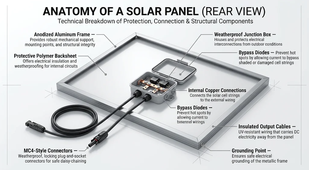
Output cables with weather resistant insulation and standard connectors, such as the MC4 connector common on modern panels, link panels together and to the rest of the system. A secure, sealed electrical enclosure matters because panels sit outdoors for decades.
What Are Solar Cells Made Of?
A crystalline silicon solar cell is made of a thin silicon wafer, doped with boron and phosphorus to form a p n junction, plus a textured surface, thin antireflective and passivation coatings, and metal contacts. The cell is the light converting part, so its materials differ from the glass, polymers and aluminum that make up the rest of a panel.
The main parts of the cell are:
- Silicon wafer: the base, doped one way (boron for p type or phosphorus for n type), with a thin layer on one side doped the opposite way to create the junction.
- Textured surface: a chemically etched surface that increases how much light enters the wafer, according to the DOE.
- Antireflective coating: bare silicon is shiny. Ossila says it can reflect up to about 35 percent of light. A thin coating, commonly silicon nitride, cuts that loss and gives cells their dark blue or black color.
- Passivation layers: very thin layers, such as silicon nitride, aluminum oxide or silicon oxide, that reduce the loss of electrical charges at the surfaces.
- Metal contacts: silver, and in some designs aluminum or copper, collect the current.
A single cell makes only about 1 or 2 watts, according to the U.S. Energy Information Administration. Manufacturers connect dozens of cells into a module to reach a useful voltage and power. If someone asks what a solar cell is made of in a thin film panel, the answer changes to layers such as cadmium telluride or CIGS instead of a silicon wafer.
What Is a PV Cell Made Of?
A PV cell is made of a semiconductor, usually silicon, arranged as p type and n type regions that meet at a junction, with metal contacts on the front and back and thin surface layers that reduce reflection and charge loss. The physics of how light creates a current in this structure was covered in the solar cells section above.
From the sunny side down, a typical crystalline silicon PV cell contains:
- Front metal fingers and busbars.
- An antireflective and passivation coating.
- A thin n type layer.
- The p n junction.
- A thicker p type base.
- A rear passivation layer and rear metal contact.
Some designs reverse the polarity and use an n type base. Light is absorbed in the silicon, the junction separates the freed electrons, and the metal contacts collect them.
It is easy to confuse the related terms:
- PV cell: one individual device that converts light to electricity.
- PV module (solar panel): many cells connected and laminated under glass, with a frame and junction box.
- PV array: a group of modules wired together.
- PV system: the array plus inverters, wiring and often batteries.
AGHow has a related guide that explains this in more detail, What Is a PV Cell?.
Are All Solar Panels Made of the Same Materials?
No. Most panels share the same glass, polymer and aluminum, but the cell materials and cell designs differ. The most important distinction is between technologies that use different semiconductors and designs that are different ways of building a crystalline silicon cell.
| Technology | Main semiconductor | Basic construction | Important material differences | Typical use | Key advantages and limits |
|---|---|---|---|---|---|
| Monocrystalline silicon | Crystalline silicon (single crystal) | Wafers cut from a Czochralski ingot, with doped regions, coatings and contacts | The mainstream wafer type, p type or n type | Residential, commercial, utility | High efficiency and long life, but rigid and needs purified silicon |
| Polycrystalline silicon | Crystalline silicon (many grains) | Cells from cast silicon blocks | Same module materials as mono | Older and some budget systems | Historically lower cost, but lower efficiency and now a small share |
| Thin film | CdTe, CIGS or amorphous silicon | Thin layers deposited on glass, plastic or metal | Cadmium and tellurium (CdTe), indium and gallium (CIGS) | Utility scale, some flexible uses | Low cost manufacturing for CdTe, but lower efficiency than silicon and needs more protection |
| TOPCon | Crystalline silicon, usually n type | Silicon wafer with an ultra thin tunnel oxide layer on the rear | Same module materials, more silver per cell than PERC | Residential to utility | Efficiency about 23.5 percent for modules, with higher silver use |
| Heterojunction (HJT) | Crystalline silicon wafer with thin amorphous silicon layers | Thin amorphous silicon layers on both sides of the wafer | Typically also uses transparent conductive layers; more silver than TOPCon | Premium and bifacial products | Similar efficiency to TOPCon, but the highest silver use of the group |
Two points avoid common confusion. First, PERC, TOPCon, HJT and back contact are cell architectures, which are different ways of building a silicon cell. They are not separate semiconductors. The Aurora Solar article lists some of these alongside monocrystalline and thin film as if they were the same kind of choice. Second, bifacial describes a panel that collects light from both sides, usually with glass glass construction, and does not describe a different cell material.
Industry data show how fast the market is moving. The ITRPV roadmap reports that n type wafers held about 82 percent of the market in 2025, TOPCon is the leading cell technology, and PERC has fallen to roughly 14 percent. The Fraunhofer ISE Photovoltaics Report of July 2026 likewise describes the market as dominated by crystalline silicon and n type TOPCon.
Next generation designs are emerging. The DOE reports perovskite cells reaching 28 percent efficiency in the lab by 2026, but says they must survive 20 years outdoors to be commercially viable. The ITRPV expects silicon based tandem cells in considerable volumes from around 2028.
Do Solar Panels Contain Rare Earth Metals or Toxic Materials?
Conventional silicon panels are mostly glass, aluminum, silicon, polymer and copper, and none of the sources I reviewed list rare earth elements among their standard materials. Some panels do contain small amounts of lead, and some thin film panels use cadmium compounds. What a panel contains depends on its technology and manufacturer, so no sweeping statement covers every panel.
- Silicon, glass, aluminum and copper: these make up nearly all of a silicon panel by weight. The EPA describes the aluminum frame, copper wire and plastic junction box as easily recyclable.
- Silver and internal copper: present in the cell contacts. The EPA notes that panels typically contain very small amounts of both.
- Lead: crystalline modules often use solder containing small amounts of lead for connections, according to a REC Group white paper. The EPA says toxic metals such as lead and cadmium may be present in solar panels. Check the manufacturer’s datasheet or compliance declaration for a specific product.
- Cadmium and tellurium: cadmium telluride (CdTe) thin film panels contain cadmium compounds. The DOE notes that CdTe and CIGS cells need more protection than silicon to last outdoors. The EPA says at least one U.S. manufacturer runs dedicated recycling facilities for thin film panels that recover the cadmium and tellurium.
- Critical materials: the EPA lists aluminum, tin, tellurium and antimony, plus gallium and indium in some thin film modules, as critical materials that panels may contain.
- Perovskites: this is still a research technology, and many formulations contain lead. Ossila notes that some solution processed materials can generate toxic lead during processing.
On rare earth elements, the critical materials above are not rare earths, which are a specific group of 17 elements. The sources I reviewed do not list them in standard silicon or thin film modules. Rare earths are best known for magnets in other technologies, such as some wind turbines.
The practical point is end of life handling. Because toxic metals may be present, panels should be recycled or disposed of through proper channels, not thrown in general waste. Rules vary by location.
How Are Solar Panels Manufactured?
Solar panels are made by purifying silicon, growing it into crystals, slicing it into wafers, turning wafers into cells, and then laminating many cells with glass, polymers and a frame. So what materials are used to make solar panels? The raw inputs are quartz for silicon, boron and phosphorus for doping, silver and copper for contacts, glass, polymer films and aluminum.
- Raw material processing: quartz is refined into metallurgical grade silicon, which is only about 99 percent pure, according to Ossila.
- Silicon purification: the DOE describes the Siemens process, in which a silicon bearing gas passes over a heated filament and deposits high purity silicon, producing polysilicon.
- Ingot production: for monocrystalline silicon, a large crystal is pulled from molten silicon using the Czochralski process. ITRPV says this process has about 95 to 100 percent of the market.
- Wafer slicing: the ingot is cut into very thin wafers with diamond coated wire saws, which leave behind silicon sawdust called kerf.
- Solar cell processing: the wafer surface is chemically textured, doped to form a p n junction, and coated with antireflective and passivation layers. The exact steps vary with cell architecture.
- Electrical contact formation: silver paste is screen printed in a finger and busbar pattern and fired onto the cell.
- Cell interconnection: cells are soldered together with copper ribbons into strings.
- Layer stacking: the strings are laid between encapsulant films, with glass on the front and a backsheet or second glass sheet behind.
- Lamination: heat and vacuum melt and bond the film layers into one sealed unit.
- Framing and junction box installation: an aluminum frame is added and a junction box with cables is attached to the back.
- Testing and quality control: each panel is flash tested under standard test conditions of 1,000 W/m² irradiance, a 25 °C cell temperature and an air mass of 1.5, and its measured output is recorded on the datasheet.
Can Solar Panel Materials Be Recycled?
Yes, much of a panel can be recycled, especially the glass, aluminum and copper. The cells, silver and bonded polymers are harder to recover. The IRENA organization, as quoted by Resource Recycling in 2020, says at least 85 to 90 percent of a panel’s weight can be recycled in a traditional recycling facility.
The EPA says glass makes up about 75 percent of a panel and glass recycling is a well established industry. The aluminum frame, copper wire and plastic junction box are also easily recycled. What is harder:
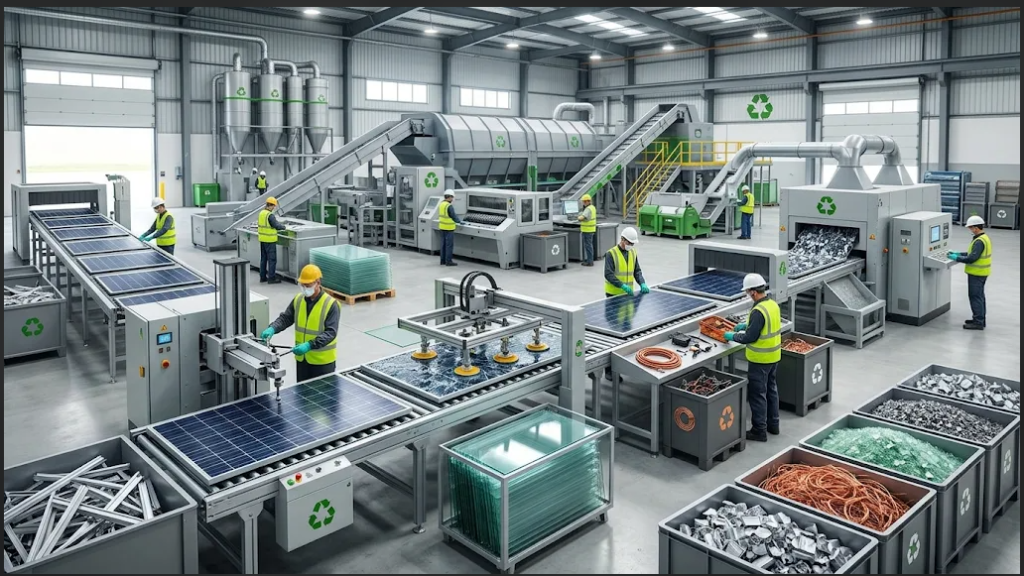
- Cell materials: silver and internal copper are valuable but exist in tiny amounts, which makes recovery difficult to justify economically.
- Bonded layers: the polymer layers that seal a panel from weather also make it hard to take apart, since high temperatures are often needed to loosen the adhesive, according to the EPA.
- Silicon: in some processes, glass, aluminum and copper are recovered and the silicon cells may be incinerated.
- Thin film: dedicated processes can recover cadmium and tellurium, the EPA notes.
Regional rules differ. In Europe, producers and importers are legally responsible for end of life management, according to REC Group. In the United States, rules differ by state, so check the EPA’s guidance and your state agency. I did not research United Kingdom or Australian rules, so check national guidance there.
End of life management matters because panels are designed to last about 25 years. The EPA’s research office expected the U.S. to have the second largest volume of PV waste, so large quantities will reach recyclers in coming decades.
Why Do Solar Panel Materials Matter for Performance and Lifespan?
Each material controls part of how much power a panel makes and how long it keeps making it. No single layer decides quality. A panel is only as durable as its weakest layer.
- Efficiency: clear glass and antireflective coatings let more light reach the cells. High quality silicon, good surface passivation and well designed contacts help turn more of it into current. Higher temperatures reduce efficiency, which is one reason the frame leaves room for airflow.
- Moisture and UV resistance: the encapsulant and backsheet or rear glass keep water and ultraviolet light away from the cells. Backsheet degradation is described as a leading cause of efficiency loss.
- Heat and mechanical strength: tempered glass and the aluminum frame resist weather and loads, while the encapsulant cushions the cells.
- Electrical safety: insulation in the encapsulant and backsheet, a sealed junction box and bypass diodes reduce shock and overheating risks.
- Degradation: the DOE says silicon modules are expected to last 25 years or more while still producing over 80 percent of their original power. Warranties commonly run 25 years, according to Aurora Solar.
Panels are normally certified against international test standards for performance and safety, and an installer can show you the certification and warranty on the datasheet.
Frequently Asked Questions
What are solar panels made of? Silicon cells, glass, an EVA or POE encapsulant, silver and copper contacts, a polymer backsheet or rear glass, an aluminum frame and a junction box. Glass is the heaviest material.
What are solar cells made of? Usually a doped silicon wafer with antireflective and passivation coatings and metal contacts. Thin film cells use semiconductors such as cadmium telluride or CIGS instead.
Is every solar panel made of silicon? No. Crystalline silicon dominates, but thin film panels use other semiconductors, and perovskite cells are still in research.
What material is used in solar panel glass? Tempered glass with high transparency, often with an antireflective coating on the surface.
Do solar panels contain silver? Yes, in small amounts in the cell contacts. At the 2025 TOPCon average of about 88 mg per cell, a module of 60 to 70 cells holds roughly 5 to 6 grams, based on my own multiplication.
Do solar panels contain rare earth metals? Not as standard materials, based on the sources I reviewed. Some thin film panels use tellurium, gallium or indium, which are not rare earths.
Are solar panels made from toxic materials? Mostly glass, aluminum, silicon and polymer, but some panels contain small amounts of lead, and CdTe thin film panels contain cadmium compounds.
Can solar panel materials be recycled? Yes, mostly the glass, aluminum and copper. Cells, silver and bonded polymers are harder.
What is the most important material in a solar panel? Silicon is what converts light to electricity, but the glass, encapsulant and backsheet decide how long the panel lasts. No layer works alone.
How long do solar panel materials last? The DOE expects silicon modules to last 25 years or more, retaining over 80 percent of power. The encapsulant and backsheet are key aging points.