
Solar panels are made by refining quartz into metallurgical grade silicon, purifying it into polysilicon, growing that polysilicon into crystal ingots, slicing the ingots into thin wafers, and turning wafers into photovoltaic cells. Factories then wire the cells together, laminate them between glass and polymer layers, add a frame and junction box, and test the finished module. Thin film panels follow a different route.
Understanding how solar panels are manufactured helps you judge quality, cost and durability. The phrase “from sand to solar panels” is a useful shortcut, but it is not literal. Ordinary beach sand cannot go into a factory and come out as a panel. Manufacturers start with very pure quartz or quartzite and spend several industrial stages removing nearly every impurity.
This guide follows that journey in order. It also explains the main panel types, what manufacturing costs actually mean, what a module is made of, and what happens to panels at the end of their life.
How Are Solar Panels Made? A Step by Step Overview
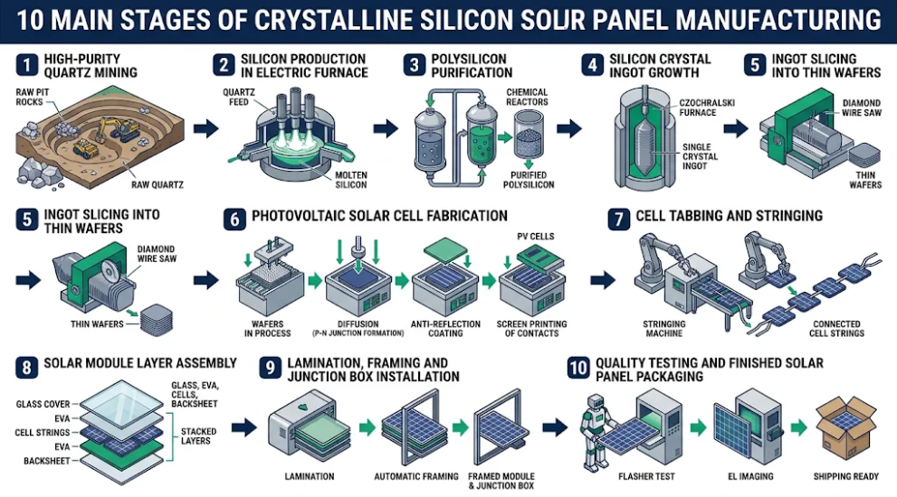
Here is how solar panels are made in ten steps for the dominant crystalline silicon route:
- Mine and select high purity quartz or quartzite.
- Heat it with carbon in an electric furnace to produce metallurgical grade silicon.
- Chemically purify it into polysilicon.
- Melt the polysilicon and grow a silicon ingot.
- Slice the ingot into thin wafers with diamond wire.
- Process each wafer into a solar cell.
- Solder cells into strings with copper ribbons.
- Stack the strings between glass and encapsulant layers.
- Laminate under heat and vacuum, then add the frame and junction box.
- Inspect, test, label and pack the finished module.
| Stage | Input | Output | Key concern |
|---|---|---|---|
| Quartz reduction | Quartz, carbon | Metallurgical grade silicon | Impurities in raw material |
| Purification | Metallurgical grade silicon | Polysilicon | Extreme purity |
| Crystal growth | Polysilicon | Ingot | Crystal quality, doping |
| Wafering | Ingot | Wafers | Thickness, breakage, kerf loss |
| Cell fabrication | Wafers | Solar cells | Efficiency |
| Interconnection | Cells | Strings | Electrical resistance, solder quality |
| Lamination and assembly | Strings, glass, encapsulant | Module | Moisture protection |
| Testing | Module | Rated product | Power and safety verification |
These stages often happen in separate factories. The U.S. Department of Energy (DOE) notes that the main silicon module manufacturing steps typically occur separately from each other, which is why a module maker may buy cells from another company.
1. Raw Materials: Starting With Silica and Quartz
Silicon is the semiconductor at the heart of most panels, but silicon does not occur as a pure element in nature. It occurs mostly as silica, which is silicon dioxide (SiO2), found in quartz, quartzite and sand. Silica contains oxygen bound to silicon, and manufacturers must remove that oxygen.
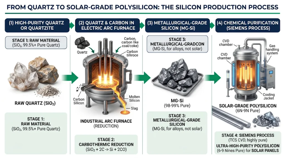
Not every sand works. Suitable material has high silica content and low levels of iron, aluminum, titanium, boron and phosphorus, because impurities later affect cell performance. For that reason producers favor selected quartz or quartzite deposits.
The silica is loaded into a submerged electric arc furnace with carbon sources such as coal, coke, charcoal or wood chips. At very high temperatures the carbon pulls oxygen away from the silica, leaving molten silicon and carbon monoxide. The result is metallurgical grade silicon. Ossila gives its purity as about 99 percent, which suits alloys and chemicals but is far from enough for photovoltaics.
2. Turning Raw Silicon Into High Purity Polysilicon
Polysilicon is a high purity, fine grained form of crystalline silicon, produced by chemically converting metallurgical grade silicon into a gas, purifying that gas, and depositing silicon back as a solid. In simple terms, the process leaves impurities behind by turning silicon into a compound that can be distilled.
DOE explains that the gases are synthesized from metallurgical grade silicon, hydrogen and chlorine. In the common Siemens process, the silicon bearing gas passes over thin silicon rods heated electrically. Silicon atoms deposit on the rod surface and the rod grows thick, forming a large U shaped polysilicon rod. The hydrogen and chlorine are reused in a closed cycle, and the filament itself is made of pure silicon so it does not contaminate the product.
The second route is the fluidized bed reactor. Small silicon beads float in an inverted cone shaped vessel while a silicon hydrogen gas is pumped in, and silicon deposits on the beads until they grow too heavy and drop to the bottom for harvesting. Siemens remains the main method: the 2026 edition of the International Technology Roadmap for Photovoltaics (ITRPV) puts its share of feedstock production at about 85 percent in 2025.
Purity matters because stray atoms act as traps where electrons are lost before they can become current. Solar grade polysilicon is commonly described as six nines pure (99.9999 percent) or better, though specifications vary by producer and cell design.
3. Growing Silicon Ingots
A silicon ingot is a large block or cylinder of solid silicon grown from molten polysilicon. How the silicon crystallizes at this stage decides whether the final panel is monocrystalline or multicrystalline.
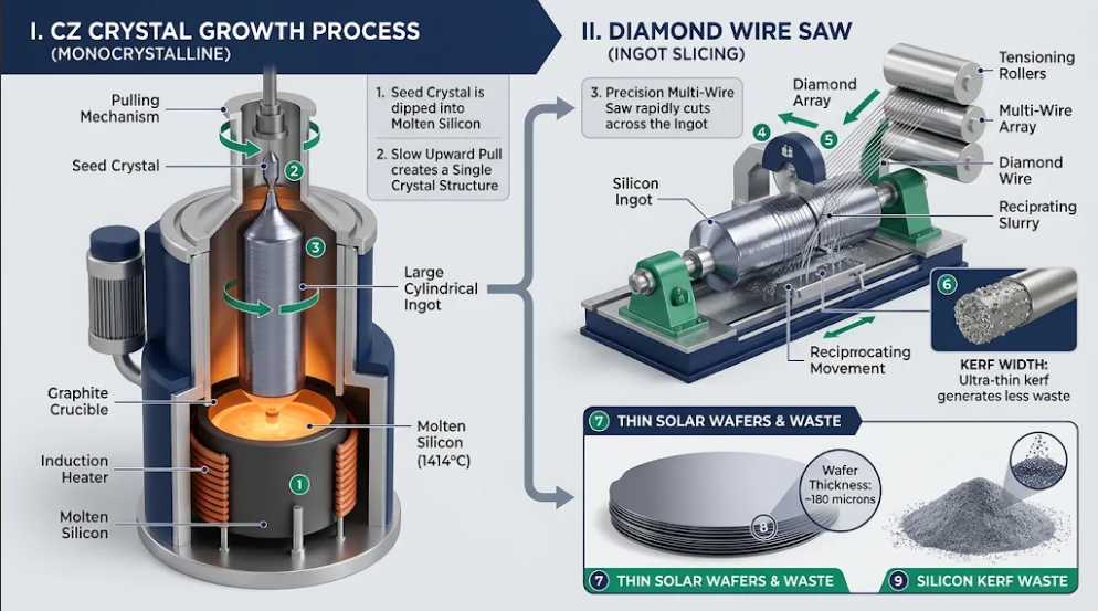
Monocrystalline ingots. Manufacturers use the Czochralski process. Polysilicon chunks melt in a quartz crucible, and dopants such as boron, gallium or phosphorus are added to set the electrical type. A small seed crystal touches the liquid surface and is pulled upward slowly, and the molten silicon follows the seed’s crystal structure, forming a large cylindrical monocrystalline ingot. Pull speed, rotation and temperature control determine diameter and defect levels. ITRPV reports that recharged Czochralski, which refills the crucible during pulling, holds roughly 95 to 100 percent of ingot crystallization.
Multicrystalline ingots. In directional solidification, the liquid mass cools slowly from the bottom up, forming a large grained multicrystalline ingot. The boundaries between grains hold back efficiency, which is one reason this route has faded in favor of monocrystalline silicon.
Ingot quality flows downstream. Oxygen content, crystal defects and doping uniformity all influence cell efficiency later. Note that ingot growth does not cut anything. Cutting is the next stage.
4. Cutting Silicon Ingots Into Thin Wafers
Wafers are made by trimming the ingot and slicing it with a wire saw. A monocrystalline cylinder is first squared off, and multicrystalline ingots are cut into bricks. Diamond coated wire saws then slice the silicon into very thin wafers.
The slicing turns part of the silicon into powder. DOE calls the silicon sawdust kerf. Kerf loss is the silicon that disappears as sawdust instead of becoming wafer, so thinner wire and thinner wafers directly reduce material cost. ITRPV notes that minimum as cut wafer thickness keeps decreasing across formats and cell technologies. This guide does not quote a single universal wafer thickness, since it differs by manufacturer, cell type and year.
Thin wafers break easily, so producers manage wire tension, coolant and handling carefully. After cutting, wafers are cleaned and inspected for cracks, thickness variation and electrical quality. Less common kerfless methods avoid sawing by pulling layers from molten silicon or depositing silicon on a template.
5. How Solar Cells Are Made From Silicon Wafers
A solar cell is made by treating a wafer so that light creates electric current and that current can be collected. The exact sequence depends on cell design, such as PERC or TOPCon, but the main steps are shared.
Texturing and cleaning. Chemical texturing removes saw damage and increases the amount of light that enters the wafer. The etch leaves a surface of tiny pyramids that trap light. This matters because bare silicon is shiny: Ossila notes it can reflect up to 35 percent of the light that hits it.
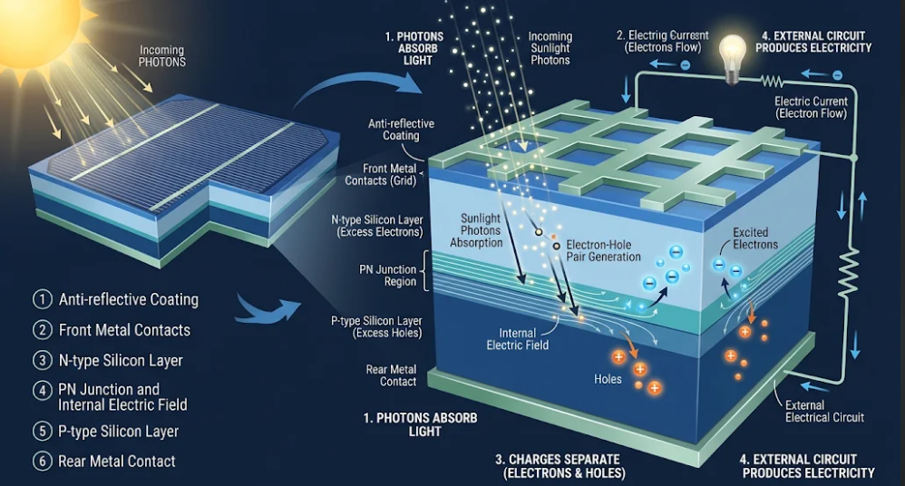
Doping and the PN junction. Pure silicon conducts poorly. Adding phosphorus creates an n type layer with extra electrons, and adding boron creates a p type layer with electron gaps. Where the two meet, a PN junction forms an electric field. When sunlight frees electrons in the silicon, that field pushes them in one direction and holes in the other, and that flow is the photovoltaic effect. Most cell types expose the wafer to a gas containing an electrically active dopant.
Passivation. Wafer surfaces have broken bonds where electrons are lost. Thin passivating layers, such as the tunnel oxide and doped polysilicon layers in TOPCon cells, calm those surfaces and keep electrons available.
Anti reflective coating. A thin dielectric coating, commonly silicon nitride, reduces reflection and gives cells their blue or black look.
Metallization. Screen printing of silver metallization for contacts is very common among cell types. Printed lines called fingers collect current and wider busbars gather it from them. Silver is costly, so manufacturers are working on thinner lines and copper alternatives. After printing, a furnace fires the metal into contact. ITRPV reports that laser enhanced contact optimization is increasingly used on TOPCon lines to lift efficiency. Finished cells are measured and sorted by performance.
6. Connecting Solar Cells Through Tabbing and Stringing
One cell produces only a small voltage, so cells must be wired together. Solder plated copper ribbons connect the silver busbars on the front of one cell to the rear of the next in a process called tabbing and stringing.
Connecting cells end to end is a series connection, which adds their voltages. Several strings are then linked, often in parallel, to reach the module’s target current and voltage. Many modern modules use half cut cells to reduce resistive loss, thin round wires instead of flat ribbons, shingled overlaps, or back contact cells where all wiring sits on the rear. Layout choices vary by manufacturer.
7. Assembling the Solar Panel Module
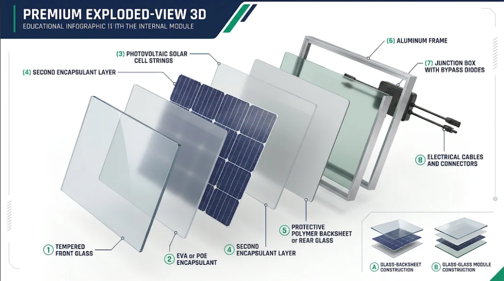
A module is a weatherproof package of connected cells with a protective front, back, frame and electrical outlet. The interconnected strings are placed face down on glass covered with a sheet of polymer encapsulant, a second encapsulant sheet goes on top, then a tough backsheet or another sheet of glass. Seen from the sun side, the order is glass, encapsulant, cells, encapsulant, then backsheet or rear glass.
Each layer has a job. Tempered glass protects against hail and passes light. Encapsulant such as EVA or POE bonds the layers, cushions the cells and keeps out moisture. The backsheet or rear glass adds electrical insulation and a moisture barrier. The frame gives rigidity and mounting points, and the junction box holds the electrical outlet and bypass diodes.
8. Lamination, Framing, and Sealing
Lamination bonds the stack into a single sealed unit. The layered stack enters a laminator, where heat and vacuum remove air and cure the encapsulant so it flows around the cells and crosslinks. Per DOE, the stack is laminated in an oven to make the module waterproof, then fitted with an aluminum frame, edge sealant and a junction box.
The seal protects the cells from moisture, which can corrode metal contacts and reduce power over time. The junction box connects ribbons to diodes that prevent backward flow of electricity, and cables with connectors leave the box so modules can link to each other.
Two main constructions exist. A glass backsheet module has glass on the front and a polymer sheet on the back, which keeps it lighter and cheaper. A glass glass module has glass on both sides, which offers a stronger moisture barrier and rigidity, with more weight. Encapsulant choice often follows this: EVA is long established, while POE is often chosen for its moisture performance in glass glass and n type designs.
9. Solar Panel Quality Control and Testing
Factory quality control and formal certification are different things, and mixing them up is common. Routine QC is what a plant does to every module or sampled batches. Certification is a type approval of a product design by an independent lab.
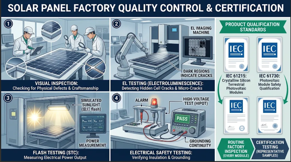
Inline QC. Visual inspection checks glass, frame and soldering. Electroluminescence (EL) imaging runs current through the module so cracks and broken contact lines show up as dark areas. Flash testing measures power under a short pulse of simulated sunlight. Standard test conditions (STC) mean 1,000 watts per square meter, a 25 degrees Celsius cell temperature and an air mass of 1.5. Insulation and ground continuity tests check electrical safety, and modules are sorted into power bins.
Certification. IEC 61215 covers performance durability and IEC 61730 covers electrical safety, and a module needs both to be considered fully qualified. The durability sequence includes thermal cycling, humidity freeze, damp heat and hail impact among others. IEC itself does not attest conformity; independent certification bodies provide that service. These tests are run on sample modules of a design, not on every unit shipped. Regional programs add requirements, such as Australia’s Clean Energy Council accreditation. Some buyers also ask for extended reliability tests, such as potential induced degradation testing.
10. The Finished Solar Module: Ready for Installation
The finished module gets a label showing its rating, usually peak power at STC in watts, plus open circuit voltage, short circuit current, and the voltage and current at maximum power. A 600 watt rating means the module produces 600 watts under STC, not that it does so all day.
Efficiency is peak power divided by the incoming light power over the module area. For example, a module of about 2.58 square meters that delivers 581 watts at STC has an efficiency of 581 divided by (1,000 times 2.58), roughly 22.5 percent. This is an arithmetic illustration, not a specific product.
A module is also not a solar power system. DOE lists the full system as modules, racking and wiring, power electronics and monitoring. Modules are packed in cartons, stacked on pallets and shipped to distributors or installers.
How Are Different Types of Solar Panels Manufactured?
| Monocrystalline silicon | Multicrystalline silicon | Thin film (CdTe) | |
|---|---|---|---|
| Starting point | Polysilicon | Polysilicon | Coated glass and semiconductor materials |
| Crystal step | Czochralski ingot | Directional solidification ingot | None, deposition of thin layers |
| Cell formation | Wafer processed into a cell | Wafer processed into a cell | Layers scribed by laser into connected cells |
| Facility model | Several separate plants | Several separate plants | Typically one facility from start to finish (DOE) |
| Market position | Dominant | Rarely quoted for homes today (SolarReviews) | Roughly 5 percent of the market (Intersolar) |
Thin film is not made by the quartz to wafer sequence. CdTe manufacturing starts with float glass carrying a transparent conductive layer, deposits the absorber by close spaced sublimation, uses laser scribing to form the cell strips and interconnects, then applies ribbons, encapsulant, a second glass sheet and a junction box. Estimates of thin film share vary from about 2 to 5 percent depending on source and year, since ITRPV puts crystalline silicon at about 98 percent.
Newer cell technologies, by maturity:
- TOPCon: commercially established and the leading cell type. ITRPV reports it led the market in 2025 and expects it to hold about half the market by 2036.
- Heterojunction (HJT): commercial, with a smaller share, using thin silicon layers on both sides of the wafer.
- Back contact: commercial and growing. ITRPV predicts up to 28 percent share for back contact cells over the next decade.
- Perovskite: still emerging. The Fraunhofer ISE Photovoltaics Report (July 2026) says perovskite on silicon tandems reach up to 35 percent in the laboratory, and ITRPV expects silicon tandems to enter mass production after 2027. Stability and lead content remain concerns.
How Much Does It Cost to Manufacture Solar Panels?
There is no single cost per panel, because “cost” changes with who is counting and where. Manufacturing cost is what it costs a factory to make a module. Wholesale price is what the factory charges. Retail price adds distribution and margin. Installed system price adds inverters, racking, labor, permits and more. Mixing them produces misleading numbers.
What the evidence shows, by definition:
| Figure | What it is | Region and year | Source |
|---|---|---|---|
| About $0.09 per watt | Average module spot price | Global, end of 2025 | ITRPV |
| Under $0.10 per watt | Module prices | Global, 2024 | IEA PVPS via pv magazine |
| About $0.11 per watt in China vs $0.30 to $0.33 in the US | Module prices | 2026 | GreentechLead (secondary source, treat with caution) |
As arithmetic only, a 600 watt module at $0.09 per watt would sell for around $54 wholesale. That is a market price, not a cost. The IEA reports that the top ten manufacturers lost USD 4.5 billion in 2024, which suggests many sold at or below cost during the price slump. No verified, comparable factory gate cost per panel was found, so none is stated here. Installed system prices belong in a separate article.
What drives manufacturing cost:
- Raw materials: polysilicon, silver paste, solar glass, aluminum and encapsulant. Silicon use per watt has fallen as wafers got thinner.
- Energy: polysilicon purification and crystal growth are very energy intensive, so electricity prices matter.
- Machinery and automation: factories are capital heavy, and equipment depreciation sits in the cost.
- Labor: a smaller share than many assume. A 2013 NREL and MIT study found production scale, not cheaper labor, explained China’s advantage at that time. This is historical and should not be read as current cost.
- Scale and yield: larger plants and lower breakage and cell loss reduce cost per watt.
- Technology and efficiency: higher efficiency spreads material cost over more watts.
- Location and supply chain: an earlier IEA study found China’s costs were 10 percent lower than India, 20 percent lower than the US and 35 percent lower than Europe, and the IEA reports China supplied about 80 percent of modules and 90 percent of wafers and polysilicon in 2024.
- Logistics and trade policy: shipping, tariffs and local content rules change landed cost.
What Materials Are Used to Make Solar Panels?
| Component | Material | Function |
|---|---|---|
| Front cover | Tempered, low iron solar glass | Protects cells and passes light |
| Solar cells | Crystalline silicon, doped, with ARC and passivation layers | Convert light to electricity |
| Contacts | Silver paste or copper | Collect current from the cell |
| Interconnects | Solder coated copper ribbon or wire | Link cells into strings |
| Encapsulant | EVA or POE | Bonds layers, cushions cells, blocks moisture |
| Rear layer | Polymer backsheet or glass | Insulates and seals the back |
| Frame | Anodized aluminum | Strength and mounting |
| Junction box | Plastic housing with bypass diodes | Electrical outlet and shade protection |
| Cables and connectors | Copper conductor, polymer insulation | Link modules together |
Mass is dominated by glass and aluminum. For a roughly 11.6 kg module, Fraunhofer CSP data show glass at 67.5 percent of weight, the frame 12.7 percent, silicon cells 2.7 percent and silver just 0.03 percent.
Is Solar Panel Manufacturing Environmentally Friendly?
Solar manufacturing has real environmental costs, but panels repay their manufacturing energy quickly. Making polysilicon and growing crystals takes large amounts of electricity, so the carbon footprint depends heavily on the local grid. Chemical handling, especially chlorosilanes and etching chemicals, requires strict controls, and Siemens plants recycle hydrogen and chlorine in a closed loop.
On emissions, the IEA found the emissions intensity of manufacturing halved since 2011, while total emissions nearly quadrupled as production expanded. On payback, Fraunhofer ISE reports energy payback time of around 1 year depending on location, and a lifespan of about 20 years in its assessment, so panels generate many times the energy used to make them. Many warranties run 25 years or more, but actual lifespan varies.
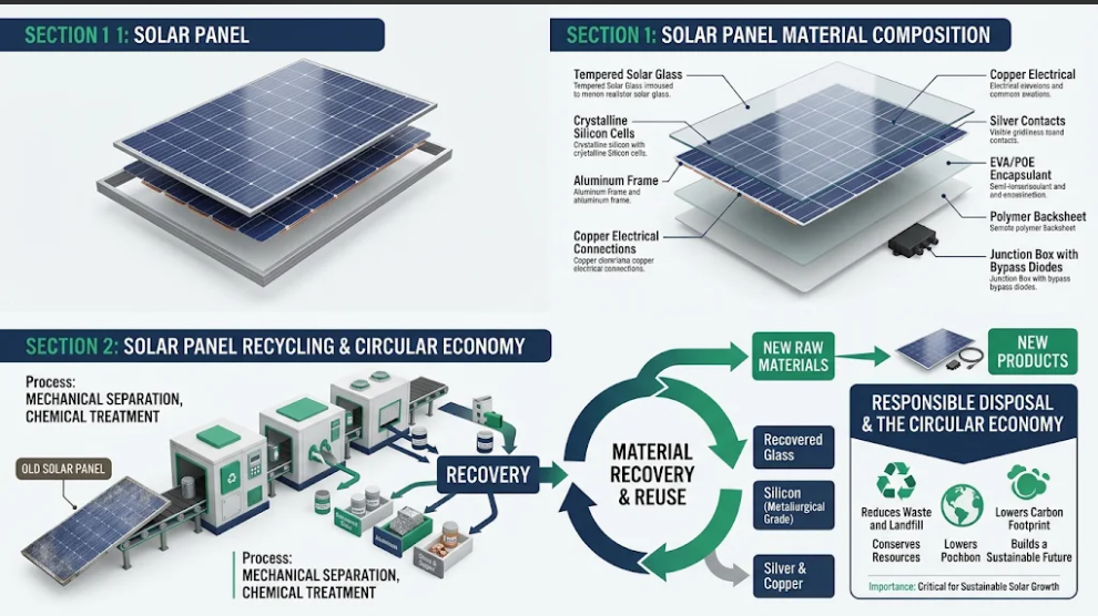
Recycling. IRENA’s July 2026 report says end of life solar waste could exceed 200 million tonnes by 2050 and that recovered material could include glass, silicon, aluminum, silver and copper. Glass and aluminum are the easy bulk materials. Silver recovery above 90 percent is possible with thermal routes, but EVA and backsheets still lack economically viable recycling and are usually burned for energy. Silver is only 0.03 percent of module mass but can be worth more than the other recovered materials combined. Recycling is technically possible, but economics and collection systems still vary by region.
Frequently Asked Questions
How are solar panels made step by step?
Quartz becomes metallurgical grade silicon, then polysilicon, then a crystal ingot, then wafers, then cells. Cells are wired into strings, laminated with glass and encapsulant, framed, fitted with a junction box and tested.
Do solar panels really start with sand?
Only loosely. The raw material is silica, but manufacturers choose high purity quartz or quartzite, not ordinary beach sand.
How is a solar cell made?
A silicon wafer is textured, doped to form a PN junction, passivated, coated to reduce reflection, and printed with metal contacts, then tested and sorted.
What is polysilicon in solar panels?
It is highly purified silicon used as feedstock for ingots. It is usually made by the Siemens process or in fluidized bed reactors.
How long does it take to manufacture a solar panel?
There is no authoritative single figure. Lamination takes minutes, but the whole chain from quartz spans several factories and often several weeks including shipping.
What materials are needed to make solar panels?
Silicon, glass, aluminum, copper, silver, polymer encapsulant, a backsheet or second glass sheet, and electronic parts in the junction box.
How much does it cost to make a solar panel?
It varies by region, technology and year, and published prices are not factory costs. Check whether a figure is cost, wholesale price, retail price or installed price.
Are all solar panels made from silicon?
No. About 98 percent of production is crystalline silicon, but cadmium telluride thin film is a commercial alternative.
What is the difference between a solar cell and a solar module?
A cell is a single semiconductor device generating a small voltage. A module is many cells wired, encapsulated, framed and fitted with an outlet.
How are solar panels tested before shipping?
Visual inspection, EL imaging, flash testing and insulation checks are common. Formal IEC testing is done on sample designs, not each unit.
Can solar panel manufacturing waste be recycled?
Some can. Silicon kerf and cell scrap can be reprocessed in principle, though economics vary. End of life modules can recover glass, aluminum and silver.
Are solar panels environmentally friendly to manufacture?
They have real manufacturing impacts but pay back their energy in roughly a year in typical conditions, and recycling is improving.